Table of Contents (click to expand)
A semiconductor is a material that imparts current, but only partially. Its conductivity lies between a conductor, which has full conductivity, and an insulator, which has negligible conductivity. Your computer or the beloved smartphone on which you are reading this right now is actually powered by a bed of silicon covered with billions of transistors thinner than a strand of hair, composed of a solid substance called a semiconductor.
A semiconductor is a material that imparts current, but only partially. Its conductivity lies between a conductor, which has full conductivity, and an insulator, which has negligible conductivity.
Your computer or the beloved smartphone on which you are reading this right now is actually powered by a bed of silicon covered with billions of transistors thinner than a strand of hair, composed of a solid substance called a semiconductor.
Recommended Video for you:
What Is A Semiconductor?
Energy Bands And The Flow Of Electricity
Any crystal is comprised of atoms that accommodate electrons in a large number of closely spaced energy levels. However, according to Pauli’s exclusion principle, the proof of which goes beyond the scope of this article, demands that only two electrons spinning in opposite directions can harbor a single energy level, making it truly stable.
These levels can be represented by lines separated by small distances where electrons are permitted to be located, in these particular levels only. A few energy levels are then grouped together to form ‘bands’, known as energy bands. The energy band below has the least amount of energy and is termed the valence band, while the energy band above it has a higher energy level and is the conduction band. The energy required for an electron to ‘jump’ this distance is called the band gap energy.
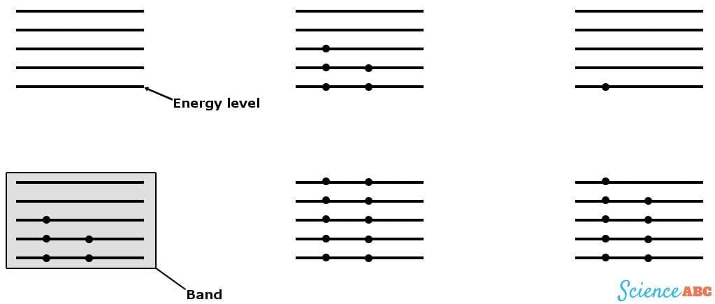
The first crystal in the diagram has an odd number of electrons in its valence band and no electrons in the next band, which makes for a single, loose electron in its highest energy level. This will readily flow to the conduction band when given a small kick or connected to a battery, providing a huge current. This crystal is a conductor; examples of conductors are metals, such as Copper and Iron.
The electrons of the second crystal are not only very stable and tied to each other, but there is also a pair of electrons in its conduction band too, thus making the flow of electrons to the conduction band nearly impossible. This represents an insulator. Paper, rubber and glass are some common insulators.
The third crystal has a loose electron, but not an empty conduction band. However, it does contain half-filled energy levels that can accommodate more electrons. This loose electron can be projected to the conduction band when given a strong enough kick, rendering a small amount of current. This crystal is a semiconductor; major examples are Silicon and Germanium.

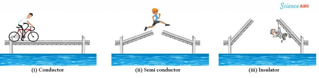
This operation can be summarized by a drawbridge analogy, where the bridges representing conductors either overlap or join so that passengers can easily cross.
Semiconductors can be represented by a poorly constructed bridge that only closes halfway and requires a passenger to jump the distance between them. Finally, an insulator is a bridge that does not close at all, making it impossible for any passenger to leap and reach the other side.
What Makes A Semiconductor So Special?
Conductivity Due To The Flow Of Positive Charges
The ability to permit the flow of electrons through a substance is its conductivity. The conductivity of conductors is highest, while it is lowest for an insulator, as the electrons flowing through it are negligible. However, as the name suggests, the conductivity of a semiconductor is moderate.
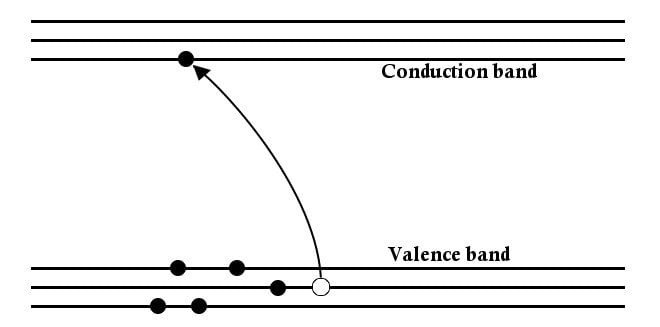
Another interesting thing about a semiconductor is that the current is carried not only by electrons, but by the vacancies they leave behind, which are known as holes. The holes left behind in the valence band can be occupied by electrons from lower states and contribute to the flow of current, thereby leaving a hole in these deeper states as well, which will be occupied by electrons beneath, and so on.
The current can thus be defined as the rate of flow of these ‘positive’ charges.
Doping And The Control Of Current Through A Device
To contemplate its utility, one must understand that the current flowing through a semiconductor, unlike a conductor, is not an uncontrollable surge of electrons, but rather a delicate combination of charges and their steady flow. Innovative engineering put forward the idea of contaminating a silicon or germanium atom on purpose to induce new energy levels.
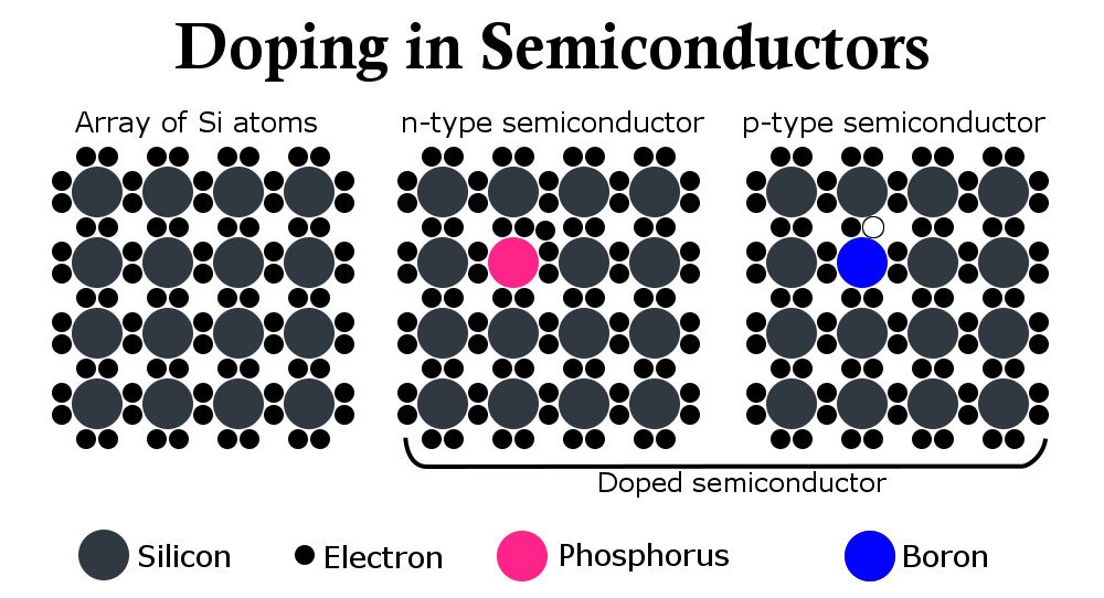
Materials are contaminated with either crystals that contain more valence electrons than a semiconductor (usually phosphorus), which tend to roam freely in the structure and contribute to the flow of electricity, or with crystals containing fewer electrons (aluminum), which borrow electrons from silicon and leave behind extra holes. The contaminated silicon resulting from the sprinkling of phosphorus is called an ‘n’ type semiconductor and the resulting silicon from the latter process is called a ‘p’ type semiconductor. The amount of contamination or doping provides the means of controlling current.
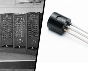
An Electronic Milestone: The Transistor
The unique properties of semiconductors led engineers to produce tiny devices that control the flow of current through a circuit. This device, known as a transistor, has changed the course of humanity since its invention in 1947.
The disturbance causing electrons to jiggle and jump can also be brought about by subjecting semiconductors to high temperatures. Thus, these materials possess a dual nature of behaving as conductors at these high temperatures and insulators at lower temperatures (less jiggling). Transistors are widely used as switching devices and amplification devices in wireless communication technologies.
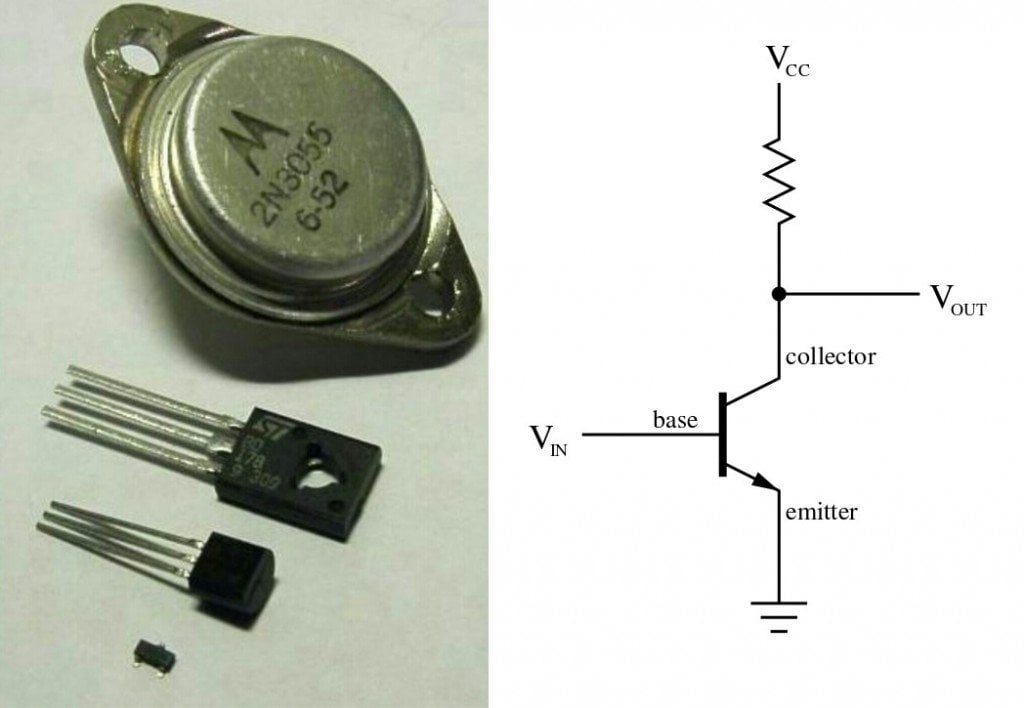
A transistor is made by either sandwiching a p-type material between two n-type materials or sandwiching an n-type material between two p-type materials.
Like the knob on top of a tap, the voltage applied to the p-type material controls and governs the current that flows from the largely doped n-type material to the relatively less doped n-type material on the opposite side. The current that is allowed to flow is interpreted as logic ‘1’, while no current is known as logic ‘0’, thus converting them to binary digits, the language of computers. The transistors switch between these ones and zeroes, and feeds to another circuit as an input made up of similar transistors, resulting in a sequence of outputs – again, ones and zeroes. An exquisite visual explanation of transistors work can be found here.
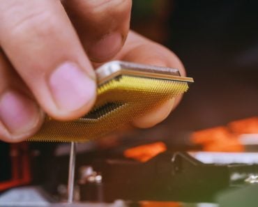
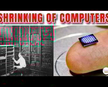
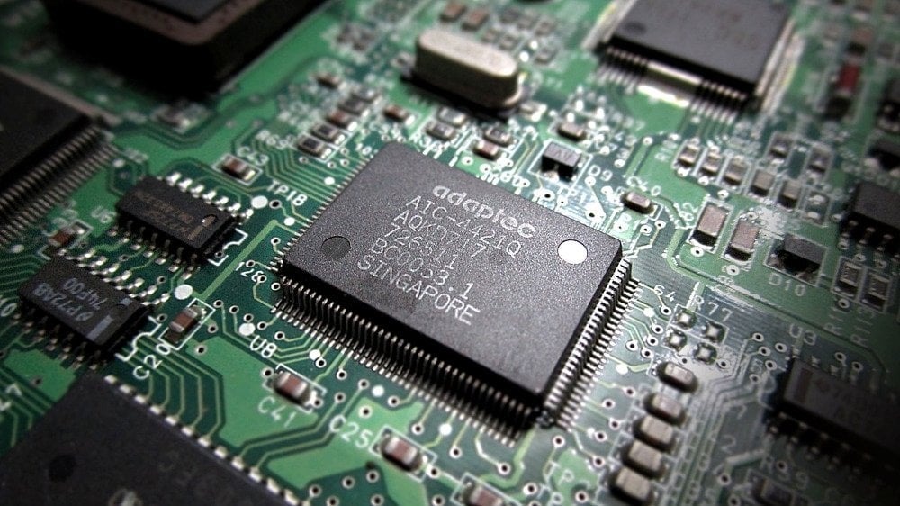
These switches are the building blocks of logic gates, which are in turn the building blocks of a microprocessor, the brain of your computer, and now our mobile phones too. Advanced technologies have aided the reduction and scaling down of the size of transistors to nano-meters, according to Moore’s Law, which allow for a billion of them to be crammed onto a tiny silicon chip. Claustrophobia is the least of their concerns.
This is a huge advantage and it is no exaggeration that these materials have revolutionized the technological world. The transistor is easily one of the most important inventions of the last century, as the modern world is dependent on and shaped by semiconductor technologies. This is especially true when it comes to integrating radio, TV, e-mail and dozens of other separate technologies into a single five-inch cuboid and connecting people on a global scale!